
Intel EMIB-T Explained: Intel's Answer to CoWoS
5/29/2026

Intel EMIB-T is the upgraded silicon-bridge packaging technology Intel built to crack open the AI accelerator market that TSMC's CoWoS platform has dominated. Here is how it works, how it compares, and why investors should care.
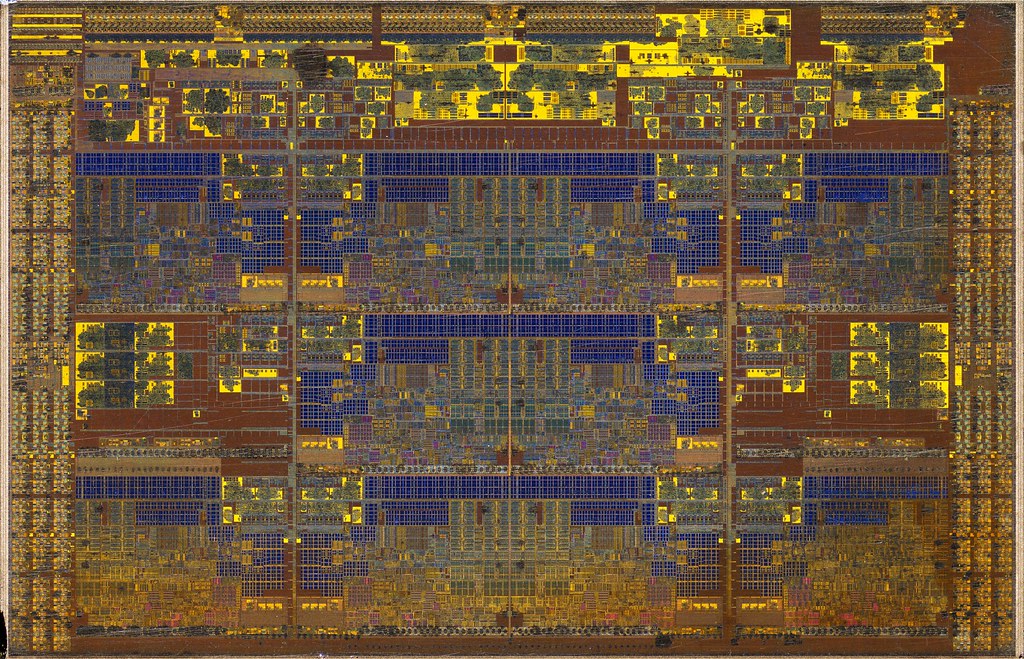
What Is Intel EMIB-T?
EMIB-T (Embedded Multi-die Interconnect Bridge with TSVs) is the next evolution of Intel's EMIB packaging, unveiled at the Electronic Components Technology Conference (ECTC) in May 2025 and heading toward fab rollout in 2026. The "T" stands for through-silicon via, the single biggest change versus standard EMIB. Where original EMIB routes signals around a tiny silicon bridge buried in the substrate, EMIB-T punches vertical connections straight through that bridge, unlocking the power delivery and bandwidth that modern AI accelerators demand.
If you are new to the underlying concept, it helps to start with the original technology. We covered the fundamentals in Intel EMIB Explained: The Chip Tech Taking on CoWoS. The short version: instead of placing every chiplet on one massive, expensive silicon interposer (the CoWoS approach), Intel embeds small silicon bridges only where two dies need to talk. EMIB-T keeps that elegant idea but removes the ceilings that kept plain EMIB out of the highest-power AI sockets.
In plain terms, EMIB-T is Intel's purpose-built answer to a simple market reality: the world cannot get enough AI packaging capacity, almost all of it runs through TSMC's CoWoS, and chip designers are desperate for a credible second source. EMIB-T is engineered to be that second source.
Why Does Advanced Packaging Suddenly Matter for AI?
For decades, the headline in chips was the transistor node - 7nm, 5nm, 3nm. The race was about cramming more transistors onto a single die. But a modern AI accelerator like an NVIDIA GPU is no longer one chip. It is a system in a package: one or more compute dies sitting next to several stacks of high-bandwidth memory (HBM), all wired together with thousands of ultra-short, ultra-fast connections.
That wiring is the job of advanced packaging. And it has quietly become the tightest chokepoint in the entire AI supply chain. You can have the best 3nm GPU die in the world, but if you cannot package it together with HBM at scale, you cannot ship it.
Three forces made packaging the new battleground:
- The memory wall. AI models are starved for memory bandwidth more than raw compute. HBM stacks sit physically next to the GPU, and connecting them requires dense, short interconnects only advanced packaging can provide. We dug into the memory side of this in DRAM vs. NAND: Understanding the 2026 AI Memory Bottleneck.
- The end of easy die shrinks. As single-die scaling slows and gets pricier, chipmakers stitch together multiple smaller chiplets. That makes the interconnect between chiplets as important as the chiplets themselves.
- Reticle limits. Lithography can only print a die up to roughly 858 mm2 (the reticle limit). To build something bigger, you must combine multiple dies in one package, which again means packaging.
This is why a packaging acronym most investors had never heard of is suddenly a stock-moving topic. Whoever supplies packaging capacity supplies the AI boom.
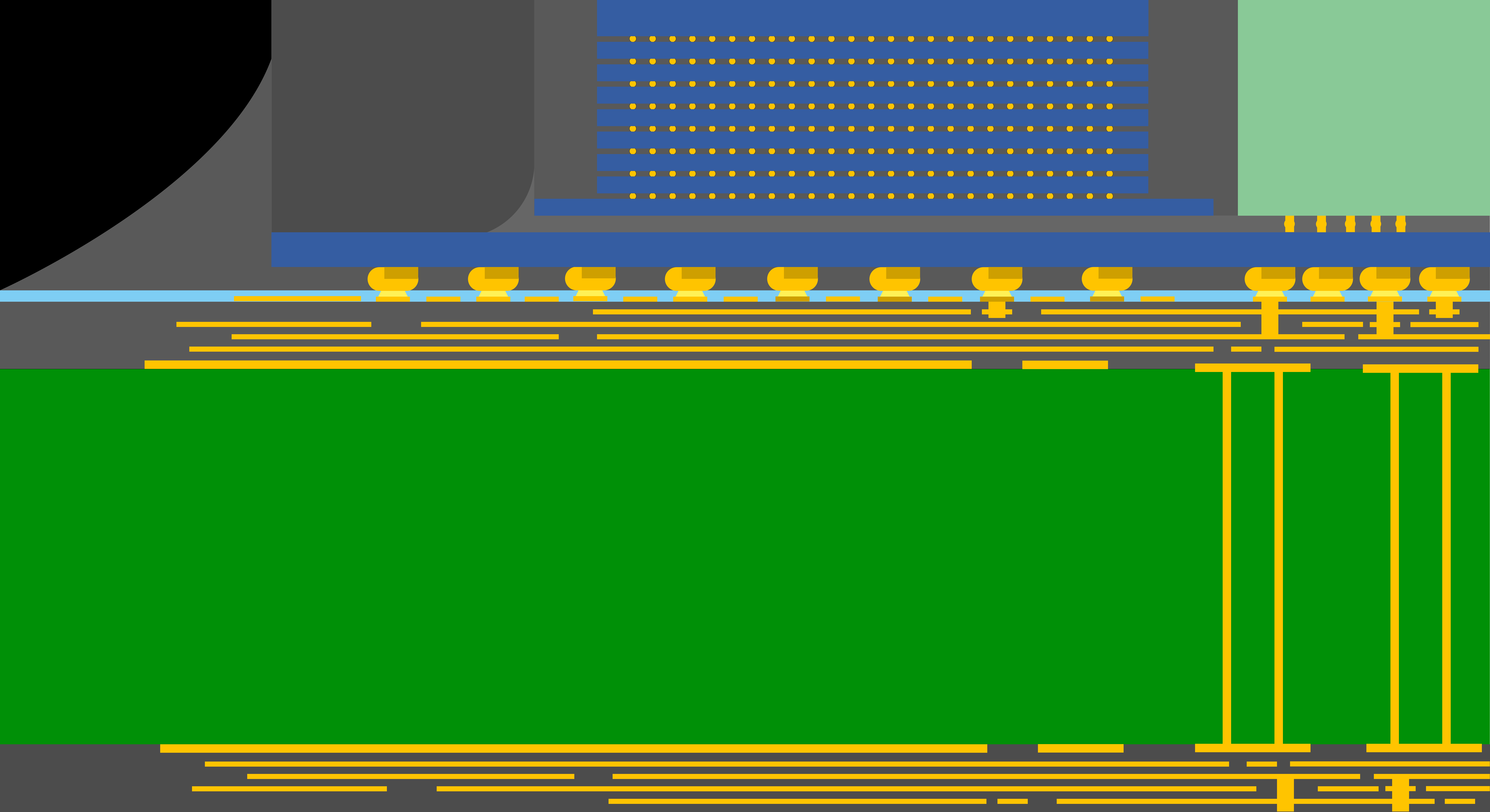
How EMIB-T Actually Works
To understand why EMIB-T is a genuine leap and not a marketing rebrand, it helps to break down the three engineering upgrades Intel disclosed at ECTC 2025.
1. Through-Silicon Vias (TSVs) for vertical power and signal
Standard EMIB had a problem: the silicon bridge sat in the way of vertical connections, so power and some signals had to route around it. That is fine for moderate workloads but becomes a bottleneck for a 1,000-watt AI accelerator. EMIB-T drills TSVs straight through the bridge, allowing power and high-speed signals to pass vertically. This is what finally makes the bridge compatible with HBM4-class power delivery and the high pin-count UCIe interface.
2. Metal-Insulator-Metal (MIM) capacitors for clean power
High-speed chiplet links are extremely sensitive to power noise. A momentary voltage dip can corrupt data. Intel integrated MIM capacitors directly into the bridge to act as tiny local energy reservoirs, smoothing out voltage and keeping signal integrity high even as data rates climb past 32 Gb/s per pin on the UCIe-A interconnect.
3. A copper ground plane grid for isolation
Pack thousands of fast signals close together and they start interfering with each other (crosstalk). EMIB-T adds a copper ground plane grid that isolates signals from one another, which is essential as bandwidth and density scale up. Together, these three additions let one EMIB-T bridge do what a section of a full CoWoS interposer does, but only in the spots where it is actually needed.
The net result, per Intel's disclosures, is a bridge that supports HBM4 and HBM4e memory at data rates of 32 Gb/s per pin or higher, alongside Intel's Foveros 3D stacking (which uses sub-10 micron copper-to-copper hybrid bonding) for vertical compute integration. EMIB-T handles the lateral, 2.5D connections; Foveros handles the vertical, 3D ones.
EMIB-T vs. TSMC CoWoS: The Head-to-Head
This is the comparison that matters. TSMC's CoWoS (Chip-on-Wafer-on-Substrate) is the incumbent that packages nearly every leading AI accelerator today. The fundamental architectural difference is simple: CoWoS uses one large silicon interposer for everything; EMIB-T uses small embedded bridges only where dies meet.
| Attribute | Intel EMIB-T | TSMC CoWoS |
|---|---|---|
| Core structure | Small silicon bridges embedded in organic substrate | Large continuous silicon interposer under all dies |
| Interposer cost | Lower (uses silicon only where needed) | Higher (full wafer-scale interposer) |
| Warpage / thermal mismatch | Reduced (less large-area silicon, lower CTE mismatch) | More sensitive at very large sizes |
| Yield at huge package sizes | More predictable (defect in one bridge is localized) | A single interposer defect can sink a big part |
| Bandwidth density per link | Very high with TSVs; routing area still smaller than full interposer | Extremely high; mature, dense routing |
| Latency | Slightly higher (longer transmission paths in some layouts) | Slightly lower |
| Maturity / track record | EMIB shipping for years; EMIB-T ramping 2026 | Industry standard, years of high-volume AI production |
| Capacity (2026) | New capacity coming online; Amkor partnership adds flexibility | ~130,000 wafers/month target, still oversubscribed |
The honest summary: CoWoS is the more mature, slightly higher-performance platform, and it is not going away. But EMIB-T is competitive on bandwidth, potentially cheaper, and architecturally better suited to the enormous package sizes the next generation of AI chips will require. For chip designers, the deciding factor in 2026 may be less about a few percent of latency and more about one word: availability.
Why the CoWoS Bottleneck Is Intel's Opening
EMIB-T would be a footnote if CoWoS had spare capacity. It does not. This is the single most important business fact in the whole story.
Here is the supply-and-demand picture the industry has reported:
| CoWoS metric | 2024 | 2025 | 2026 (projected) |
|---|---|---|---|
| TSMC monthly capacity | ~35,000 wafers/mo | ~75,000 wafers/mo | ~130,000 wafers/mo |
| Total global CoWoS demand | ~370,000 wafers | ~670,000 wafers | ~1,000,000 wafers |
TSMC has roughly doubled CoWoS output two years running and demand still outruns it. By 2026, NVIDIA alone is projected to need around 595,000 CoWoS wafers, about 60% of total global demand, with AMD taking roughly another 11%. When the two largest AI chip designers absorb the lion's share of a sold-out platform, everyone else, from hyperscalers building custom ASICs to second-tier accelerator startups, is left hunting for an alternative.
That alternative is exactly the gap EMIB-T is designed to fill. As reporting from Tom's Hardware noted, EMIB-T is heading for fab rollout specifically as CoWoS capacity remains limited. Intel does not have to beat CoWoS on every spec. It just has to be good enough and available when CoWoS is not.
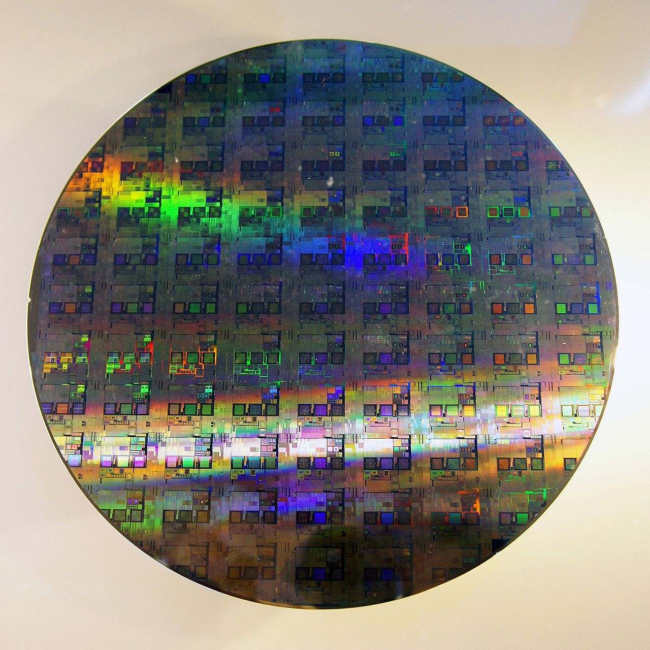
How Big Can EMIB-T Scale?
One of EMIB-T's most striking selling points is sheer size. Because a localized bridge defect does not ruin an entire interposer, Intel argues EMIB-based packages can grow far larger with more predictable yields. The company has laid out an aggressive roadmap.
| Year | Package size | Reticle multiple | HBM stacks | Compute tiles | EMIB bridges |
|---|---|---|---|---|---|
| Today | Single reticle (~858 mm2) | 1x | Limited | 1-2 | Few |
| 2026 | 120 x 120 mm | ~8x | Up to 12 | Several | 20+ |
| 2028 | 120 x 180 mm | ~12x+ | 24+ | Up to 16 | 38+ |
To put that in perspective, a 120 x 180 mm package is roughly the footprint of a smartphone, and Intel has shown concepts with up to 16 compute tiles and 24 HBM sites on advanced 18A and 14A nodes, even floating future HBM5 integration. This is system-level integration at a scale that is genuinely hard to do with a single monolithic interposer. If AI accelerators keep getting bigger, and every roadmap says they will, the architecture that scales most gracefully has a structural advantage.
What Does This Mean for Intel (INTC) Investors?
This is where the engineering meets the income statement. Intel's turnaround story has two engines: its logic foundry (the 18A and 14A process nodes) and its packaging business. The catch is that logic takes years to ramp and prove out yields, while packaging can generate revenue much sooner.
The numbers show why this matters. Intel Foundry generated only about $307 million in external revenue last year against a roughly $10.3 billion operating loss, and Q1 2026 external foundry revenue was reported around $174 million. That is a tiny external business relative to the ambition. Advanced packaging, where Intel already has a real, shipping track record, is widely seen as the fastest on-ramp to external AI revenue, likely before 14A logic contributes meaningfully.
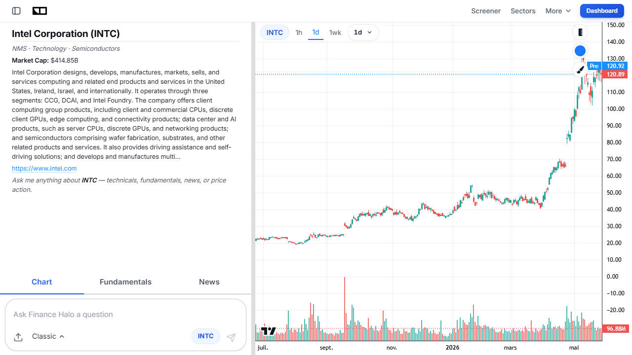
Sentiment around INTC has been volatile. Under CEO Lip-Bu Tan, the stock staged a dramatic rally on the back of cost cuts, a reported NVIDIA equity tie-up, a Google ASIC deal, and 18A reaching volume manufacturing. But the rally pushed shares well above the analyst consensus target, and the rating distribution skews heavily toward "Hold." In other words, the market has already priced in a lot of optimism, which raises the bar for execution.
For investors, the practical takeaway is to separate the narrative ("Intel will challenge TSMC in AI packaging") from the numbers (external revenue is still small, and meaningful packaging dollars are a late-2026-into-2027 story). If you want to dig into how to value a turnaround like this rather than chase the headline, our guide on how to analyze a stock before buying walks through the framework, and our piece on what counts as a good P/E ratio by industry is useful context when a stock is priced for a turnaround that has not fully arrived. You can also analyze INTC with Finance Halo's AI assistant to get an instant read on technicals and fundamentals.
Real-World Example: SK hynix, Amkor, and the CoWoS Scramble
The clearest proof that EMIB-T is more than a slide deck came from the market's reaction to two concrete developments.
The SK hynix test. In May 2026, reports surfaced that SK hynix, the world's leading HBM supplier, was testing Intel's 2.5D EMIB packaging for HBM integration amid TSMC CoWoS tightness. SK hynix shares jumped to record highs on the news. Why does a memory maker testing a packaging technology move stocks? Because it signals that the HBM ecosystem is actively validating Intel as a real alternative supply path, not just kicking the tires. If the company that makes the memory is willing to qualify EMIB, accelerator designers have cover to follow.
The Amkor partnership. Intel also teamed up with Amkor Technology, a leading outsourced assembly and test (OSAT) provider, to offer EMIB packaging. This matters because it adds capacity and flexibility. Designers worried about single-sourcing from Intel's own fabs get a second venue, which lowers the perceived risk of committing to EMIB-T.
Put these together with the underlying math, NVIDIA reserving roughly 60% of 2026 CoWoS supply, and you get a textbook market opening: a sold-out incumbent, a credible challenger with a real product, a marquee memory partner validating it, and an OSAT partner adding capacity. That is the bull case for Intel packaging in one paragraph. The bear case is equally simple: TSMC is doubling CoWoS every year, EMIB-T still has to prove high-volume yields, and none of this produces large revenue overnight.
Who Else Wins From the Packaging Shift?
EMIB-T is an Intel story, but the packaging bottleneck is an industry-wide theme, and several tickers are leveraged to it. Thinking in terms of the whole value chain is often more profitable than betting on a single name.
- TSMC (TSM): Still the dominant winner. Even with EMIB-T competing, TSMC is selling every CoWoS wafer it can build. A second source relieves pressure but does not dethrone the leader. You can pull up TSM on Finance Halo to see how the market is valuing the packaging king.
- NVIDIA (NVDA): The biggest consumer of packaging. More total industry capacity, from any vendor, helps NVIDIA ship more GPUs. A credible EMIB-T option is a mild positive for the whole accelerator complex. Compare the demand side by analyzing NVDA's setup.
- SK hynix and the HBM makers: HBM is the scarce ingredient packaging exists to connect. More packaging capacity means more HBM gets consumed, a tailwind we explored in the 2026 AI memory bottleneck guide.
- Amkor (AMKR) and OSATs: Direct beneficiaries of packaging demand spilling beyond TSMC's walls.
- Intel (INTC): The highest-risk, highest-variance play, levered to whether EMIB-T converts technical promise into real foundry revenue.
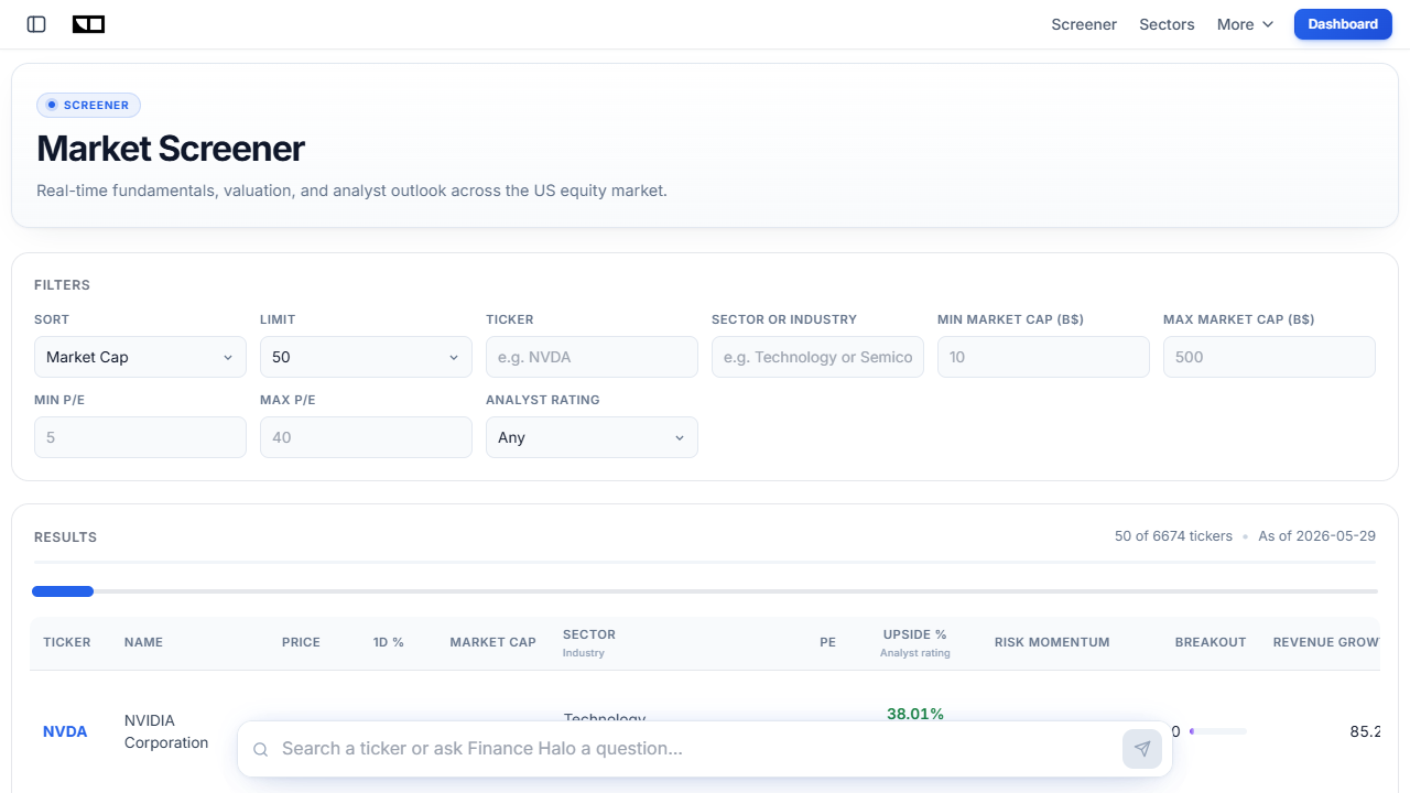
To compare valuations across these names side by side, screen them with real fundamentals on the Finance Halo market screener and rank by P/E, market cap, and sector before you commit capital.
Common Mistakes Investors Make With Packaging Plays
- Mistake 1: Confusing a tech win with a revenue win. EMIB-T being technically impressive does not mean it is profitable yet. Always check whether external revenue is actually flowing. Fix: read the segment numbers in the 10-Q, not just the press release.
- Mistake 2: Treating it as a binary "Intel beats TSMC" bet. Both can win as the whole pie grows. The packaging market is expanding fast enough to support a strong incumbent and a credible number two. Fix: think in terms of total capacity growth, not market share zero-sum.
- Mistake 3: Chasing the news pop. Stocks like SK hynix and INTC have spiked on packaging headlines. Buying after a 200%+ run, above analyst targets, is a different risk profile than buying the theme early. Fix: respect valuation and your entry price.
- Mistake 4: Ignoring the timeline. EMIB-T ramps in 2026 with meaningful revenue more likely in 2027-2028. Impatient capital gets shaken out. Fix: match your holding period to the technology's actual ramp schedule.
- Mistake 5: Forgetting the memory and equipment links. The bottleneck touches HBM makers and packaging-equipment suppliers too. Fix: map the full value chain before picking one name.
- Mistake 6: Over-concentrating in one ticker. A single execution stumble can hit any one company hard. Fix: spread exposure across the theme and size positions sensibly.
Frequently Asked Questions
What does EMIB-T stand for?
EMIB-T stands for Embedded Multi-die Interconnect Bridge with through-silicon vias (TSVs). It is Intel's upgraded version of EMIB that adds vertical TSV connections, MIM capacitors, and a copper ground grid so the silicon bridge can support high-power HBM4 memory and the high-bandwidth UCIe interface.
Is EMIB-T better than TSMC's CoWoS?
It depends on the metric. CoWoS is more mature and offers slightly lower latency, while EMIB-T can be cheaper, reduces warpage at very large sizes, and scales to bigger packages with more predictable yields. For many designers in 2026, EMIB-T's biggest advantage is simply being available while CoWoS is sold out.
When will EMIB-T be available?
Intel disclosed EMIB-T at ECTC in May 2025 and is targeting fab rollout in 2026. Industrial deployment and meaningful customer volume are expected to build through 2026 into 2027 and 2028, alongside Intel's 18A and 14A process nodes.
Why is advanced packaging such a big deal for AI?
Modern AI accelerators are systems in a package: a compute die surrounded by stacks of HBM memory. Connecting them with dense, short, high-speed links is the job of advanced packaging, and that capacity, not raw transistor count, has become the tightest bottleneck in the AI supply chain.
Does EMIB-T mean I should buy Intel (INTC) stock?
Not automatically. EMIB-T is a genuine technical asset and Intel's fastest path to external AI revenue, but Intel Foundry's external revenue is still small and the stock already rallied sharply on turnaround optimism. Evaluate the valuation, the execution timeline, and your own risk tolerance. This article is educational, not investment advice.
What is the difference between EMIB-T and Foveros?
EMIB and EMIB-T handle 2.5D lateral connections, wiring chiplets and memory side by side. Foveros handles 3D vertical stacking, placing one die directly on top of another using copper-to-copper hybrid bonding. Intel uses them together: Foveros for the vertical compute stack and EMIB-T for the lateral links to HBM.
Who are the main beneficiaries of the CoWoS shortage?
TSMC still captures most demand, but the shortage pushes designers toward alternatives like Intel's EMIB-T and OSAT partners such as Amkor. HBM makers like SK hynix benefit from any expansion in total packaging capacity, since more packaging means more memory consumed.
How much CoWoS capacity does NVIDIA use?
By 2026, NVIDIA is projected to require around 595,000 CoWoS wafers, roughly 60% of total global demand of about 1 million wafers, with AMD taking around 11%. That concentration is precisely why other chip designers are looking for a second packaging source.
Conclusion
Intel EMIB-T is the clearest sign yet that the AI chip war has moved from the transistor to the package. By adding TSVs, MIM capacitors, and a copper ground grid to its embedded silicon bridge, Intel turned EMIB from a clever interconnect into a legitimate contender for the high-power AI accelerator sockets that TSMC's CoWoS has owned. The architecture's lower interposer cost, reduced warpage, and graceful scaling to 120 x 180 mm packages with 24+ HBM stacks give it a real structural case.
The three things to remember: first, the CoWoS bottleneck is the opening, with demand projected at 1 million wafers in 2026 and NVIDIA alone absorbing about 60% of it. Second, packaging is Intel's fastest on-ramp to AI revenue, well ahead of its logic nodes, which is why the SK hynix test and Amkor partnership moved markets. Third, narrative is ahead of numbers: external foundry revenue is still small, and the real payoff is a 2027-2028 story, so respect valuation and timeline before chasing the theme.
Whether you are weighing INTC, TSM, NVDA, or the broader packaging ecosystem, the smart move is to compare them on fundamentals rather than headlines. For the macro backdrop on sector rotation and where AI capital is flowing, read today's AI-generated market intelligence report, or start screening the semiconductor names directly.
Try it yourself: Analyze INTC with Finance Halo's AI assistant to get instant price targets, technical analysis, and investment insights in seconds.
Disclaimer: This article is for educational purposes only and does not constitute investment advice. Always do your own research before making investment decisions.