
Intel EMIB Explained: The Chip Tech Taking on CoWoS
5/28/2026

Intel's Embedded Multi-die Interconnect Bridge - known as EMIB - is quietly reshaping how AI chips are built, connecting separate silicon dies with a precision that rivals the best packaging technology on the market. As TSMC's CoWoS lines stay chronically oversubscribed and Nvidia locks up the lion's share of available capacity, EMIB is emerging as the technology that could break the packaging bottleneck holding back the next wave of AI accelerators.

What Is Intel EMIB, and Why Does It Matter?
EMIB stands for Embedded Multi-die Interconnect Bridge. It is a 2.5D advanced packaging technology developed by Intel that uses small pieces of silicon - called bridges - embedded inside cavities in an organic package substrate. These bridges create short, high-density electrical pathways between multiple chiplets or dies sitting side by side in the same package.
The problem EMIB solves is fundamental to modern chip design. For decades, chipmakers squeezed more transistors onto a single monolithic die by following Moore's Law - doubling transistor density roughly every two years. But as process nodes shrink below 5nm and die sizes push against the physical limits of lithography (the so-called reticle limit, roughly 858 mm2), building everything on one slab of silicon becomes economically and physically impractical.
The alternative is chiplets: designing a complex chip as a collection of smaller, specialized dies that are packaged together. A CPU die, a memory die, an I/O die, and an AI accelerator die can each be optimized on the best process node for their function, then connected in the same package. This sounds simple, but the hard part is the connection. Die-to-die links must be fast, dense, low-latency, and energy-efficient - and that is precisely where Intel EMIB shines.
A Technology Born Out of Packaging Necessity
Intel introduced EMIB into volume production in 2017. The original application was connecting High Bandwidth Memory (HBM) stacks to a host processor without using a large and expensive silicon interposer. Instead of running signals through a costly interposer that spans the entire package, EMIB places a tiny silicon bridge only where the dies need to talk to each other - right at the edge between them. The rest of the substrate remains organic, which is cheaper and easier to manufacture at scale.
Why Packaging Is Now the Performance Bottleneck
As transistor scaling has slowed, the bottleneck in building faster chips has shifted from logic density to memory bandwidth and die-to-die communication. An AI accelerator that runs at petaflop speeds is useless if it cannot feed data to its compute units fast enough. Advanced packaging - and specifically the interconnect density it enables - has become the key variable that separates the best AI chips from the rest. EMIB is Intel's core answer to that challenge.
How Does EMIB Work? The Silicon Bridge Architecture Explained
At its core, EMIB is an elegantly simple concept executed with extreme precision. Here is how the manufacturing process works, step by step:
- Bridge fabrication: Small silicon bridge dies are manufactured on a dense process node. They contain only passive routing metal layers - no active transistors - optimized purely for high-density interconnect.
- Bridge embedding: The silicon bridges are placed into pre-defined cavities in the organic substrate using thermo-compression bonding. The bridge sits slightly below the surface of the substrate, flush with it.
- Die placement: The functional chiplets - logic dies, HBM stacks, I/O tiles - are placed on top of the substrate. Their edges overlap the embedded silicon bridges.
- Micro-bump connection: High-density micro-bumps connect the underside of each chiplet to the silicon bridge below. These bumps are far denser than the standard C4 bumps used to connect a chip to a PCB - EMIB-T targets a bump pitch of 35 micrometers, compared to 100-130 micrometers for standard bumps.
- Signal routing: Electrical signals travel from die A, down through micro-bumps, laterally through the dense metal layers of the silicon bridge, then back up through micro-bumps into die B. The path is extremely short, which keeps latency low and energy consumption per bit minimal.
What Makes Silicon Bridges Better Than Organic Routing
Organic substrates can route signals, but their feature sizes are relatively coarse - typically 2 micrometers or wider. Silicon, by contrast, can be patterned at sub-micron feature sizes using semiconductor lithography. This means a silicon bridge can carry hundreds or thousands of signal wires in a region where an organic substrate could only carry tens. The result is dramatically higher bandwidth density between adjacent dies.
EMIB vs. Full Silicon Interposer
The key architectural difference between EMIB and a full silicon interposer (as used in some implementations of TSMC CoWoS-S) is coverage. A full interposer is a large piece of silicon that spans the entire bottom surface of a multi-die package. It is expensive to fabricate because large silicon tiles have lower yield than small ones. EMIB places silicon only at the die-to-die boundaries - a fraction of the total package area. This targeted approach preserves most of the cost advantage of organic substrates while delivering silicon-grade interconnect density exactly where it is needed.
Intel EMIB vs. TSMC CoWoS: A Side-by-Side Comparison
The two dominant 2.5D advanced packaging approaches in the market today are Intel's EMIB and TSMC's CoWoS (Chip-on-Wafer-on-Substrate). They share a common goal - connecting multiple dies with high-bandwidth, low-latency links - but they take meaningfully different architectural paths to get there.
| Feature | Intel EMIB | TSMC CoWoS-S | TSMC CoWoS-L |
|---|---|---|---|
| Interposer type | Embedded silicon bridges only | Full silicon interposer | RDL carrier + embedded silicon bridges |
| Package substrate | Organic (BGA) | Organic (via interposer) | Organic (via RDL) |
| Max reticle scale (2026-27) | 8-12x (EMIB-M) | ~3.3x | ~3.5x |
| Bump pitch (next-gen) | 35 microns (EMIB-T) | ~45-55 microns | ~45-55 microns |
| HBM4 compatibility | Yes (EMIB-T, 2025) | Yes (CoWoS-S N+1) | Yes |
| Manufacturing cost | Lower (less silicon area) | Highest (full silicon interposer) | Medium |
| Capacity availability | Expanding (Amkor partnership) | Severely constrained | Severely constrained |
| Primary current user | Intel (Gaudi, Ponte Vecchio) | Nvidia (H100, H200, B100) | Nvidia, Broadcom ASICs |
Where CoWoS Leads
TSMC's CoWoS-S, which uses a full silicon interposer, offers the highest interconnect routing flexibility. Because the entire die-facing surface is silicon, any die can communicate with any other die at silicon-grade density, not just adjacent dies. For packages where multiple HBM stacks need to share bandwidth with a central compute die, full-interposer CoWoS-S provides maximum design flexibility. Nvidia's H100 and H200 GPUs are the canonical examples - four HBM3 stacks surrounding a central GH100 die, all connected through a 814 mm2 silicon interposer.
Where EMIB Has the Edge
EMIB's targeted bridge architecture wins on three dimensions: cost, yield, and scalability. Because EMIB uses much less silicon per package, manufacturing yield is higher - a defective bridge affects only the bridge's small area, not a large interposer tile. At the ultra-large package sizes needed for future AI accelerators - packages larger than a smartphone - building a single monolithic silicon interposer becomes practically impossible due to lithographic limits. EMIB, by using multiple small bridges at die boundaries, can scale to arbitrarily large package footprints. Intel's roadmap explicitly targets packages 12x the reticle size of today's largest AI chips, with 16 compute tiles and 24 HBM5 stacks in a single package - a scale that full-interposer CoWoS cannot match.
Which Products Use Intel EMIB Today?
EMIB is not a research project - it has been shipping in high-volume, commercially available products for nearly a decade. Here are the most significant examples:
| Product | Year | EMIB Role | Key Stats |
|---|---|---|---|
| Kaby Lake-G (with AMD GPU) | 2018 | Connects Intel CPU to AMD Radeon GPU and HBM2 | First consumer product with EMIB |
| Stratix 10 FPGA | 2017 | Connects FPGA die to HBM2 stacks | First EMIB production silicon |
| Ponte Vecchio (Data Center GPU) | 2022 | Connects 47 dies using EMIB + Foveros | 100B+ transistors, used in Aurora supercomputer |
| Sapphire Rapids (Xeon w/ HBM) | 2023 | Connects CPU die to HBM2e stacks | Up to 64 GB HBM at 1.0 TB/s bandwidth |
| Gaudi 3 AI Accelerator | 2024 | Integrates HBM2e memory via EMIB | 1.8 PFlops FP8, 128 GB HBM2e, 3.7 TB/s |
| Clearwater Forest (Xeon) | 2025 | EMIB for lateral tile integration | Compute tiles on Intel 3 + Foveros Direct |
EMIB in Client Processors
Intel has also deployed Foveros 3D stacking - a complementary packaging technology - in its Meteor Lake and Lunar Lake mobile processors. Lunar Lake (Core Ultra 200V Series, released September 2024) uses EMIB alongside Foveros to maximize interconnectivity between compute, GPU, and NPU tiles while minimizing power consumption. The combination of EMIB for lateral die-to-die connections and Foveros for vertical stacking gives Intel a uniquely flexible packaging toolkit compared to any single competitor.
Screening Semiconductor Stocks
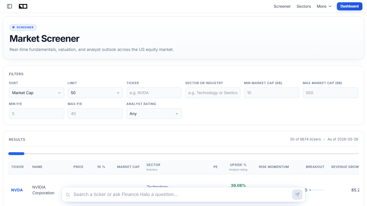
When evaluating how advanced packaging innovations like EMIB translate into investment opportunities, fundamental screening is essential. The Finance Halo screener lets you filter semiconductor names by P/E ratio, market cap, and sector in seconds - a good starting point before diving into a company's packaging roadmap.
EMIB-T: The Next-Generation Upgrade for AI Workloads
The original EMIB architecture routes signals horizontally through the bridge's metal layers, wrapping around the bridge's edges to travel from die to die. EMIB-T - where the "T" stands for TSV (through-silicon via) - adds vertical electrical connections that punch straight through the bridge die. This architectural change unlocks several capabilities that are critical for next-generation AI accelerators.
Key Technical Improvements in EMIB-T
- 35-micron bump pitch: Compared to standard EMIB bumps, the finer pitch enables roughly 2x the number of connections per unit area, directly translating to higher bandwidth between chiplets.
- HBM4 compatibility: The HBM4 standard requires power delivery and signaling that standard EMIB struggles to provide. EMIB-T's TSV architecture supports the power delivery demands of HBM4, HBM5, and future memory generations.
- UCIe support: EMIB-T supports the Universal Chiplet Interconnect Express (UCIe) standard, which enables interoperability between chiplets from different vendors - a key requirement for the open chiplet ecosystem Intel is building around its foundry services.
- Shorter signal paths: TSVs eliminate the need to wrap signals around the bridge edges, reducing latency and power consumption per bit transmitted.
EMIB-T Timeline and Commercial Impact
According to Tom's Hardware reporting, EMIB-T is targeted for production fab rollout in 2025, with initial customer sampling expected in the second half of the year. Customers for EMIB and EMIB-T packaging are expected to ramp in the second half of 2026, potentially contributing several billion dollars in packaging revenue. This makes EMIB-T the primary catalyst that could transform Intel's advanced packaging business from a supporting act into a meaningful revenue driver.
Why Has Advanced Packaging Become the New Semiconductor Battleground?
To understand why Intel EMIB matters to investors beyond just engineers, you need to understand why advanced packaging has become strategically important in the first place. The answer lies in three converging trends:
The End of Easy Scaling
Moore's Law - doubling transistor density every two years - has not died, but it has slowed dramatically. Moving from 5nm to 3nm delivers less than half the density gain that moving from 28nm to 14nm did. The cost per transistor, which fell predictably for decades, has actually risen for the most advanced nodes. This means chipmakers can no longer rely solely on shrinking transistors to improve performance. Packaging - connecting multiple optimized dies - has become the primary route to compound improvements in performance per watt and performance per dollar.
The AI Compute Explosion
Training and running large AI models requires moving enormous amounts of data between memory and compute units at very high speed. A single Nvidia H100 GPU contains 80 GB of HBM3 memory providing 3.35 TB/s of memory bandwidth - a figure that requires advanced 2.5D packaging to achieve. As AI model sizes grow from hundreds of billions to trillions of parameters, future accelerators will need even more HBM stacks, higher bandwidth, and larger die complexes. Advanced packaging is the only practical way to deliver that scale.
The Supply Constraint Reality
TSMC's CoWoS lines have been chronically oversubscribed since 2023. Nvidia alone is estimated to consume roughly 60% of global CoWoS capacity for its AI GPU products. This leaves custom ASIC vendors, AI chip startups, and hyperscaler in-house chip teams scrambling for packaging capacity. Intel's EMIB lines, by contrast, are relatively unconstrained - and Intel has partnered with Amkor Technology, the world's largest outsourced semiconductor assembly and test (OSAT) company, to expand EMIB packaging capacity further. For any company that needs advanced 2.5D packaging at scale and cannot get CoWoS allocation, EMIB is increasingly the only credible alternative.
The advanced packaging market as a whole is projected to grow at a compound annual growth rate of 9.4%, approaching $80 billion by 2030, according to industry analysis. This is the market Intel is targeting with its foundry packaging strategy.
How Does EMIB Affect Intel (INTC) as an Investment?
For retail investors watching Intel stock, advanced packaging is one of the most important - and most overlooked - dimensions of Intel's turnaround story. Here is how EMIB fits into Intel's financial picture:
The Foundry Revenue Opportunity
Intel has repositioned itself as both a chip designer and a chip foundry (Intel Foundry Services, or IFS). Advanced packaging is the part of the foundry business where Intel has the deepest existing expertise and the most differentiated technology. Intel's CFO Dave Zinsner stated at the Morgan Stanley TMT conference that IFS is "close to closing some deals that are in the billions per year" in advanced packaging alone. Intel has also publicly stated that its packaging revenue is expected to exceed $1 billion in the near term - a significant contributor to the struggling foundry segment's path to profitability.
Geopolitical Tailwinds
The U.S. CHIPS and Science Act allocated $52.7 billion for domestic semiconductor manufacturing, with advanced packaging explicitly listed as a priority technology. Intel, as the primary U.S.-based advanced packaging provider, is a natural beneficiary of this policy push. Hyperscalers and defense contractors with requirements to source packaging from U.S.-based facilities have few alternatives to Intel's EMIB lines. This geopolitical angle creates demand that is partially insulated from normal competitive dynamics.
The INTC Stock Chart: Understanding the Risk
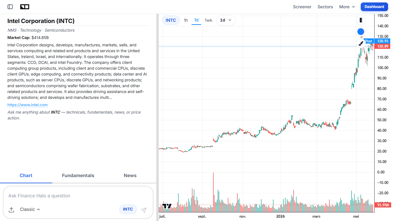
Intel's stock has faced significant pressure as the company transitions its business model, invests heavily in new fabs, and navigates manufacturing execution challenges. Before buying INTC based on an EMIB thesis, investors need to assess: is the packaging revenue opportunity large enough and near enough to matter, and can Intel execute on its foundry ramp while managing costs? For a deeper look at how to evaluate a stock like Intel before investing, see our guide on how to analyze a stock before buying.
Analyze Intel (INTC) with Finance Halo's AI assistant to get instant price targets, technical signals, and fundamental context on the packaging opportunity.
Valuation Considerations
Packaging revenue alone will not transform Intel's valuation in the short term. Intel's total revenue was roughly $54 billion in 2023 (before subsequent declines), so a $1-3 billion packaging revenue line is meaningful but not transformative unless it scales rapidly. The more important question is whether advanced packaging success validates Intel's broader foundry ambitions, attracts additional external customers, and builds the "proof of concept" that justifies the billions of dollars Intel is spending on new fabs. For context on how to use valuation metrics like P/E ratio when evaluating semiconductor stocks in transition, see what is a good P/E ratio by industry.
EMIB's Role in the AI Chip Supply Chain
The AI chip supply chain in 2025 and 2026 is defined by one overarching constraint: TSMC cannot build enough CoWoS capacity fast enough to satisfy demand. Understanding this creates a framework for evaluating who benefits from EMIB's rise:
The Winners: Companies Locked Out of CoWoS
- Custom ASIC AI chips: Hyperscalers (Google, Amazon, Meta, Microsoft) building custom AI chips often cannot get sufficient CoWoS allocation, since Nvidia has priority. For these customers, EMIB is an increasingly attractive alternative, with Intel targeting Google and Amazon specifically for packaging deals.
- MediaTek's dual strategy: MediaTek has reportedly adopted a dual packaging strategy, using both Intel EMIB and TSMC CoWoS for its AI ASIC push - a significant validation of EMIB's competitive positioning, given that MediaTek has deep relationships with TSMC.
- SK Hynix: Reports emerged in 2025 that SK Hynix - the world's second-largest memory chipmaker and the primary HBM supplier to Nvidia - is testing Intel's EMIB for HBM integration. If confirmed, this would represent a dramatic expansion of EMIB into the memory supply chain.
The Amkor Partnership: Scaling EMIB Beyond Intel Fabs
A critical strategic move Intel made was partnering with Amkor Technology to offer EMIB packaging through Amkor's OSAT facilities. This is important because it means customers who want EMIB packaging do not necessarily need to route wafers through Intel's fabs - they can access EMIB through a neutral third-party packaging house. This removes a key objection from Intel's competitors (AMD, Qualcomm) who might be reluctant to use Intel foundry services for competitive reasons but would be willing to use EMIB packaging through Amkor.
The Competitive Response from TSMC
TSMC has not stood still. In April 2026, TSMC stated that CoWoS offers the industry's largest reticle-size packaging, even as Intel EMIB rivalry intensifies. TSMC is also advancing its CoPoS (Chip-on-Wafer-on-Substrate with Photonic) technology for future optical interconnect integration. The packaging arms race is accelerating, which benefits the broader semiconductor equipment and materials ecosystem - companies like ASML, Tokyo Electron, and ASE Group that supply the tools and services needed for advanced packaging at scale.
For broader context on how sector dynamics like this play into investment decisions, read today's AI-generated market intelligence report on Finance Halo to see how semiconductor stocks and sector rotation are positioned right now.
Real-World Case Study: Ponte Vecchio and the 47-Chiplet Challenge
The most dramatic demonstration of Intel EMIB's capabilities - and its limitations - is the Ponte Vecchio data center GPU, deployed in the Aurora supercomputer at Argonne National Laboratory, which became the first U.S. exascale computer.
What Makes Ponte Vecchio Extraordinary
Ponte Vecchio, marketed as the Intel Data Center GPU Max Series, is the most complex semiconductor package ever put into volume production at the time of its launch. It integrates 47 individual chiplets into a single package using a combination of EMIB for lateral die-to-die connections and Foveros for vertical 3D stacking. The chiplets come from multiple process nodes: compute tiles on TSMC's 5nm, HBM2e memory, base dies on Intel 16, and Rambo cache tiles - all coordinated through EMIB bridges at the package level.
The Numbers
- More than 100 billion transistors in a single package
- 128 GB of HBM2e memory via eight stacks, connected through EMIB
- 3.9 TB/s of peak aggregate memory bandwidth
- Multiple EMIB bridges managing the lateral connections between HBM stacks and compute dies
- Used in the Aurora supercomputer, one of the world's fastest AI training systems
What Ponte Vecchio Proved - and What It Didn't
Ponte Vecchio demonstrated that EMIB can orchestrate multi-die complexity at a scale that no monolithic design or simpler packaging approach could achieve. It validated the technology as production-grade for the most demanding workloads in the world. However, Ponte Vecchio also came with challenges: its extreme complexity made manufacturing yields difficult to optimize, contributing to delays and cost overruns that pushed its commercial launch timeline. This is the honest trade-off of EMIB-based designs - the technology is powerful, but designing for chiplet integration and packaging yield requires engineering rigor that simpler, monolithic designs avoid.
What Gaudi 3 Refines
Intel's Gaudi 3 AI accelerator (2024) represents a more commercially-tuned application of EMIB. With 1.8 PFlops of FP8 compute, 128 GB of HBM2e at 3.7 TB/s bandwidth, and optimized HBM integration through EMIB, Gaudi 3 shows that Intel has internalized the lessons from Ponte Vecchio's complexity and produced a more manufacturable, cost-effective design. Gaudi 3 is Intel's primary weapon in the AI accelerator market against Nvidia's H100/H200, and its EMIB-based architecture is a key differentiator.
For a deeper dive into how to evaluate semiconductor stocks using fundamental metrics - including Intel's growing packaging business - the complete comparison of P/E, EPS, and PEG ratios on the Finance Halo blog is a useful reference.
Common Mistakes Investors Make When Evaluating Packaging Tech
Advanced packaging is a technically dense topic, and even sophisticated investors frequently make avoidable errors when assessing its investment implications.
- Mistake 1: Treating packaging as a commodity. Many investors assume that chip packaging is a simple, undifferentiated service - like putting a chip in a box. EMIB and CoWoS are not commodities. They require years of specialized process development, proprietary tooling, and deep co-design expertise. Assuming any OSAT can replicate Intel's or TSMC's advanced packaging in 12-18 months underestimates the moat significantly.
- Mistake 2: Equating "same technology" with "same capability." Hearing that both EMIB and CoWoS use "silicon bridges" can lead investors to assume they are equivalent. The implementation details - bridge size, bump pitch, TSV integration, substrate type, scalability limits - create very different performance and cost profiles. Always dig into the specific generation of packaging being discussed.
- Mistake 3: Ignoring manufacturing yield in the investment thesis. A packaging technology that delivers great specs on paper but has 50% yield is economically unviable. When evaluating a company's packaging strategy, ask about yield at production volumes, not just peak performance. Ponte Vecchio's yield challenges are a reminder that complexity has a cost.
- Mistake 4: Assuming CoWoS capacity constraints will resolve quickly. TSMC has been expanding CoWoS capacity since 2022, and the lines are still oversubscribed in 2025. Building new advanced packaging capacity requires specialized equipment with long lead times and extensive process qualification. Investors who expect the bottleneck to clear in one or two quarters consistently underestimate how long capacity expansion takes in practice.
- Mistake 5: Overlooking the customer lock-in dynamic. A chip designed around EMIB requires significant re-design to switch to CoWoS, and vice versa. Once a hyperscaler's custom ASIC team designs a chip for EMIB packaging, they are unlikely to switch suppliers mid-generation. This creates durable revenue relationships - but it also means early customer wins (like MediaTek or SK Hynix testing EMIB) are more strategically important than they might appear.
- Mistake 6: Ignoring the fabless angle. Fabless chip designers (AMD, Qualcomm, Broadcom, MediaTek) historically avoided using Intel for anything - it felt like feeding a competitor. The Amkor-EMIB partnership changes this calculus, because fabless designers can now access EMIB through a neutral OSAT. Investors who model EMIB adoption only from companies already using Intel fabs will underestimate the addressable market.
For more on evaluating growth companies in the semiconductor space using a disciplined framework, see the Finance Halo guide on finding deep value stocks - the same principles of rigorous fundamental analysis apply when assessing whether an investment thesis is priced appropriately.
Frequently Asked Questions
What does EMIB stand for?
EMIB stands for Embedded Multi-die Interconnect Bridge. It is Intel's proprietary advanced semiconductor packaging technology that uses small silicon bridge dies embedded in an organic package substrate to create high-density, low-latency electrical connections between multiple chiplets or dies in a single package.
How is Intel EMIB different from TSMC CoWoS?
Both technologies enable multi-die packaging with high-bandwidth die-to-die links, but they differ architecturally. TSMC CoWoS-S uses a large silicon interposer covering the entire package area, which provides maximum interconnect flexibility but at higher cost and lower yield. Intel EMIB places small silicon bridges only at the boundaries between adjacent dies, using organic substrate everywhere else - a more cost-efficient approach that also scales to larger package sizes. CoWoS-L uses a hybrid RDL carrier plus bridges, which is architecturally similar to EMIB in concept but different in implementation.
What products use Intel EMIB today?
EMIB has been in production since 2017. Products include the Stratix 10 FPGA (the first EMIB product), the Kaby Lake-G processor with AMD Radeon graphics, the Ponte Vecchio Data Center GPU (47 chiplets, used in the Aurora supercomputer), the Sapphire Rapids Xeon processor with HBM memory, the Gaudi 3 AI accelerator (1.8 PFlops, 128 GB HBM2e), and Clearwater Forest Xeon processors. More products are expected as Intel's foundry services attract external customers.
What is EMIB-T and when is it available?
EMIB-T adds through-silicon vias (TSVs) to the bridge die, enabling shorter signal paths, a finer 35-micrometer bump pitch, and full HBM4 and HBM5 memory compatibility. It also supports the UCIe chiplet interconnect standard. EMIB-T entered production fab rollout in 2025, with customer products expected to ramp in the second half of 2026.
Is Intel EMIB available through TSMC or only Intel fabs?
EMIB packaging is available through Intel's own fabs and through Amkor Technology, the world's largest OSAT (outsourced semiconductor assembly and test) company. The Amkor partnership is significant because it allows fabless chip designers who manufacture their logic dies at TSMC, Samsung, or other foundries to still access EMIB packaging through a neutral party - without sending their wafers to Intel.
Why is advanced packaging capacity so constrained right now?
The surge in demand for AI accelerators - particularly Nvidia's H100 and H200 GPUs - has overwhelmed TSMC's CoWoS packaging lines. Nvidia is estimated to account for roughly 60% of global CoWoS demand, leaving limited allocation for other customers. Building new advanced packaging capacity requires specialized equipment with 12-24 month lead times and extensive process qualification. The constraint has been building since 2022 and is expected to persist into 2026-2027, making alternatives like EMIB strategically important for the industry.
How does the CHIPS Act affect Intel's packaging business?
The U.S. CHIPS and Science Act explicitly designates advanced packaging as a national priority and allocates funding for expanding domestic advanced packaging capacity. Intel, as the primary U.S.-based provider of advanced packaging technologies like EMIB and Foveros, is a direct beneficiary. Additionally, defense and national security customers with "Made in USA" requirements for sensitive semiconductor supply chains have limited options outside Intel for advanced packaging, creating captive demand.
Should I buy Intel stock because of EMIB?
EMIB represents a genuine technological and business strength for Intel, but it should not be evaluated in isolation. Intel faces significant execution risks in its fab ramp, competitive pressure from TSMC and Samsung, and a challenging path to foundry profitability. Advanced packaging could be a multi-billion dollar revenue contributor, but Intel's overall financial recovery depends on many factors beyond packaging alone. Use Finance Halo's INTC analysis tools to evaluate the full picture before making investment decisions. This article is not investment advice.
Conclusion
Intel EMIB is one of the most important - and most underappreciated - technologies in the current AI hardware boom. By embedding tiny silicon bridges directly into an organic substrate, EMIB achieves silicon-grade die-to-die interconnect density without the cost and scalability limits of a full silicon interposer. That architectural advantage positions EMIB as a credible alternative to TSMC's CoWoS at precisely the moment when CoWoS capacity constraints are creating real supply pain for AI chip developers.
The competitive picture is nuanced. CoWoS remains the dominant technology for today's highest-volume AI products, and TSMC's manufacturing expertise is formidable. But EMIB's scalability advantage at extreme package sizes, its cost efficiency, the capacity availability through the Amkor partnership, and the CHIPS Act tailwinds create a combination of technical and commercial factors that should not be dismissed. The fact that customers like MediaTek and SK Hynix are actively testing EMIB for AI ASIC designs in 2025 is a meaningful signal of real-world adoption beyond Intel's own products.
For investors, the key numbers to watch are Intel's advanced packaging revenue (targeting more than $1 billion near-term with multi-billion deal pipeline), the EMIB-T production ramp timeline in 2025-2026, and the announcement of external foundry customers committing to EMIB packaging. These are the milestones that will determine whether EMIB transforms from an internally-used competitive advantage into a significant external revenue driver for Intel Foundry Services.
Advanced packaging is the new front line in the semiconductor arms race. Understanding the technology - not just the buzzwords - is what separates investors who can evaluate these opportunities from those who cannot.
Try it yourself: Analyze Intel (INTC) with Finance Halo's AI assistant to get instant price targets, technical analysis, and investment insights on how the EMIB packaging story is reflected in the stock's current valuation.
Disclaimer: This article is for educational purposes only and does not constitute investment advice. Always do your own research before making investment decisions.